Research Interests - Gas Sensors
 |
 |
|
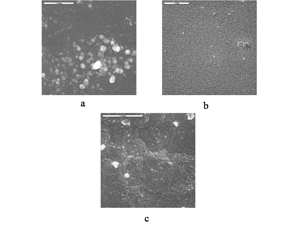
Figure 6. Scanning electron microscope
images of sensor surfaces prepared by chemical vapour deposition.
|
Figure 7. Scanning electron microscope
images of sensor surfaces prepared by screen printing.
|
|
The figures above show the difference in microstructure between sensors produced by conventional screen printed methodologies (figure 7) and those produced from chemical vapour deposition (CVD) routes (figure 6). The sensors produced from CVD routes are much thinner but also much denser. They tend to have a high surface to bulk ratio but less well developed grain boundaries and there baseline resistance is high. Overcoming this problem may lead to a new generation of sensors with enhanced sensitivity and selectivity.
|
|