|
Metal Oxide Semi Conductor Gas Sensors
Metal oxide semi conductor gas sensors are an increasingly important
technology. Most of the applications use tin dioxide or to a lesser
extent tungsten oxide devices. I am interested in using new materials
such as chromium titanium oxide (CTO) or gallium oxide for gas sensing
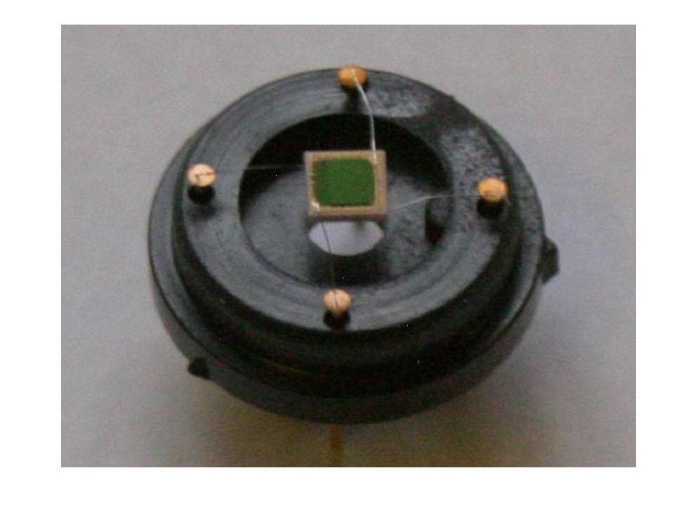
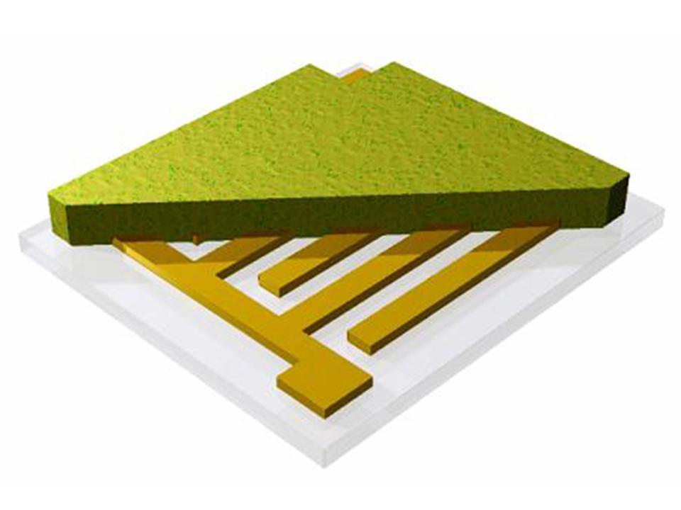
applications. Sensors are made by making inks of the sensor material
and screen printing these onto sensor chips. The sensor chips are small
alumina tiles, typically 3x3 mm square (figure 2). The coated chips
then get baked in a furnace and bound up into devices (Figure 1).
|
|
|
|
|
|
|
|
The chips are then placed in a test rig and exposed to small amounts
of test gas, typically 1 to 100 ppm in air. The test gas interacts with
the surface and causes a change in resistance accross the electrodes
which is measured by a computer and can be related to the type of test
gas and the test gas concentration.
Gas sensors of this type show great promise for use in electronic noses
and can be used for all sorts of monitoring applications from oil rigs,
food production and fire safety.
Back to top
|
|
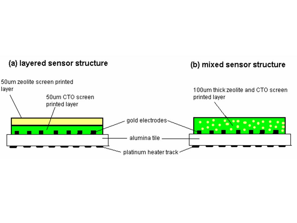
Zeolite Modified Sensors
One inherent problem with metal oxide semi conductor devices is that
they are indiscriminate, that is to say they provide a response to a
wide variety of gases. This can be a problem if we only want to measure
one specific gas, say carbon monoxide for fire safety applications.
In an effort to improve selectivity devices are modified with zeolites
(Figure 3 and 4).
|
|
|
|
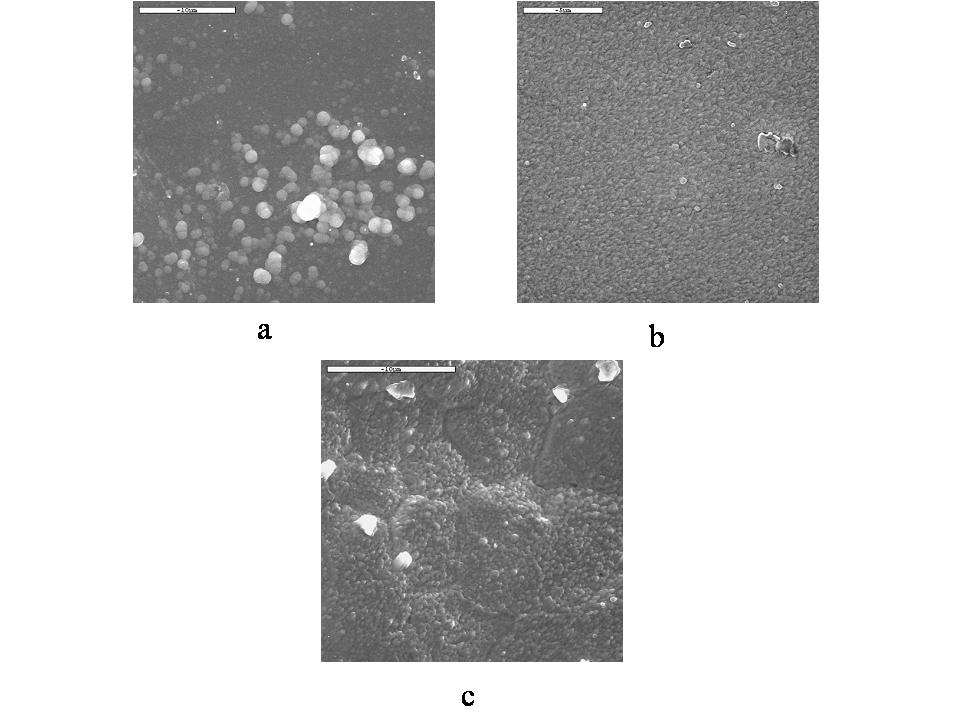
Figure 3. Cross sectional schematic
of layered and mixed sensors - explanation
|
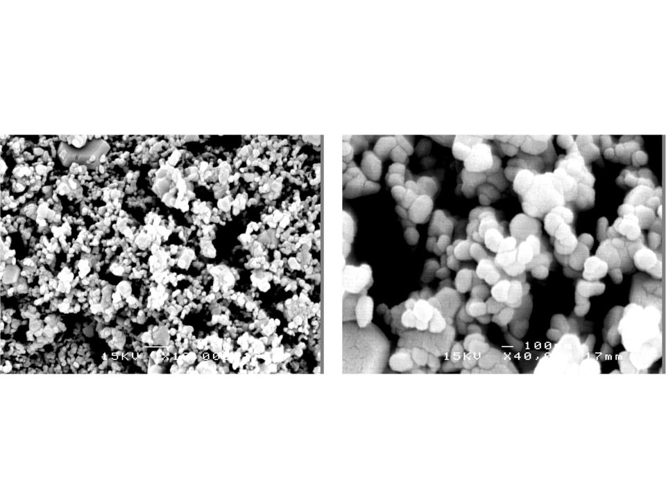
Figure 4. Scanning electron microscope
images of a layered sensor surface - explanation
|
|
The effect of a zeolite transformation layer can be
several fold. There are a variety of diffusion effects which can occur,
catalytic reactions may take place as well as the zeolite acting as
a molecular sieve and preventing large molecules getting to the sensor
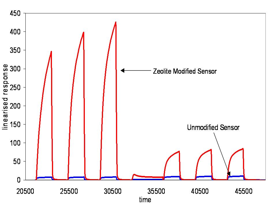
material surface. Often an enhancement in gas response is seen. Figure
5 shows an example of how a zeolite overlayer can improve the responsivity
of a CTO device by as much as two orders of magnitude.
|
|
|
Figure 5. Gas response to ethanol
of Zeolite Modified CTO Sensor and Unmodified CTO Sensor at different
gas concentrations - explanation
|
|
Different zeolite overlayers cause different effects to the measured
signal, which is in turn dependent on the gas being evaluated. In this
way the sensors become much more specific to particular gases.
Back to top
|
|
Chemical Vapour Deposition and
Gas Sensors
Another important aspect with metal oxide semi conductor gas sensors
is the sensor microstructure. All commercially produced metal oxide
semi conductor gas sensors are made using thick film technology such
as screen printing where microstructure is fairly homogenous and limited
in terms of crystallite size. CVD allows for the controlled growth of
films that have a wide variety of microstructures which may lead to
improved gas sensing properties. Figures 6 and 7 show some examples
of films grown by CVD and their screen printed versions.
|
|
|
 |
|
Figure 6. Scanning electron microscope
images of sensor surfaces prepared by chemical vapour deposition.
|
Figure 7. Scanning electron microscope
images of sensor surfaces prepared by screen printing.
|
|
explanation
Back to top
|